
I get bored easily.
 01-24-2012, 12:26 PM
#21
Boost Pope


Thread Starter
iTrader: (8)
Join Date: Sep 2005
Location: Chicago. (The less-murder part.)
Posts: 33,485
Total Cats: 6,898
The MegaSquirt design is the intellectual property of Bowling & Grippo. It would be wrong for me to build a bootleg copy of one.
You know, it's funny. I don't think I've ever used a strip board.
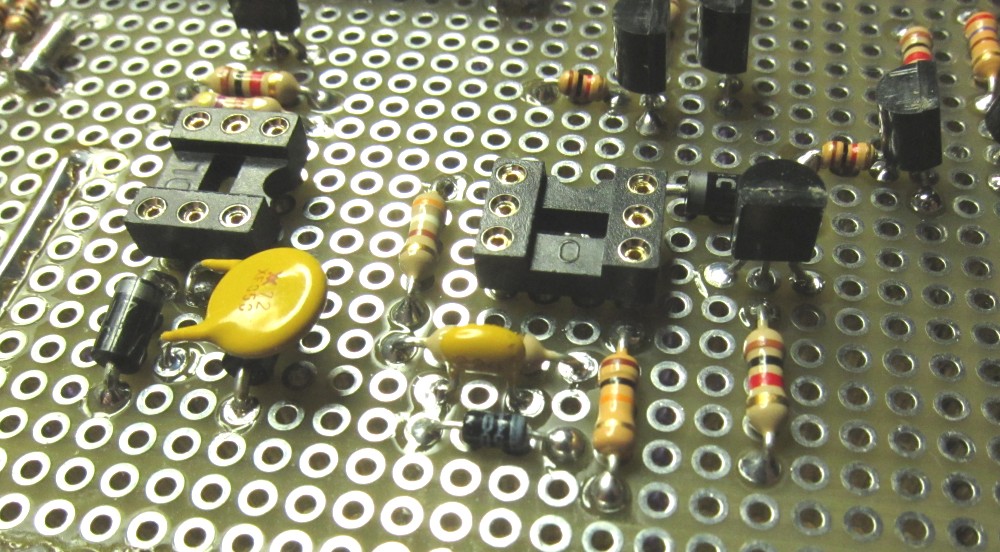
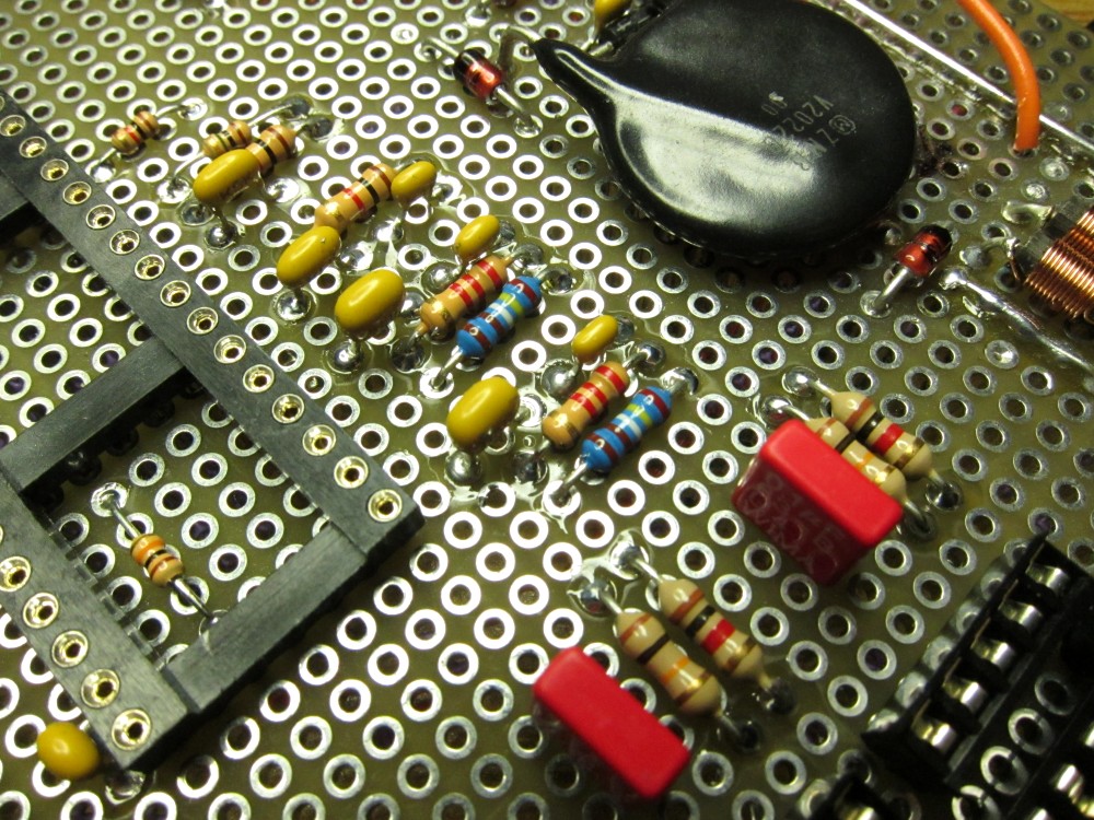
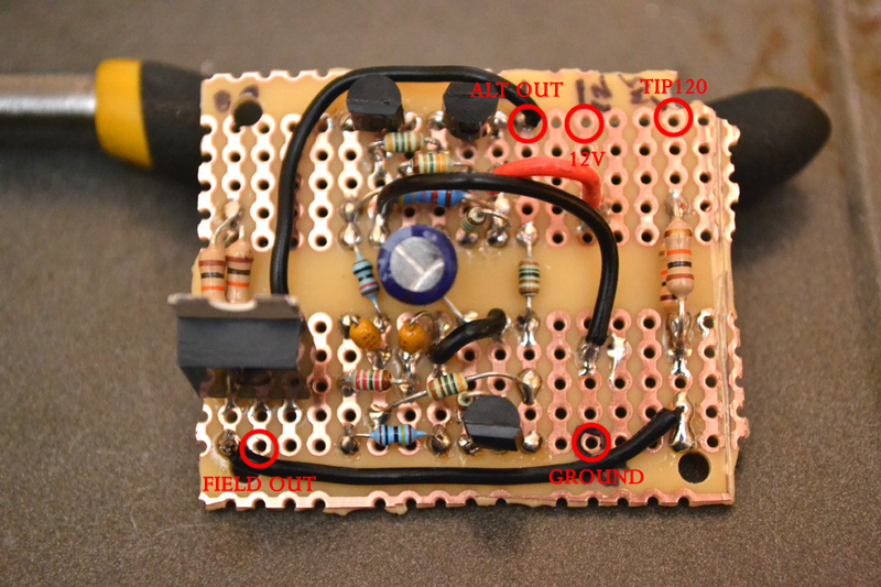
This is just a regular perfboard with copper-ringed holes, through-plated. The first pic I posted was kind of old, here's some detail showing further progress:
I made that argument rather strongly a couple of years ago, when the MS3 project was announced. I called it the "4.0" board, but essentially it would have moved the functions of the MS3X onto the main board, eliminated most of the "vintage" circuitry (the two INJ drivers presently there, the opto input, etc) and basically given you a nice package similar to an MS2 but with all the circuits you could ever need plus a better connector than a DB37.
Anyway, now we have 3.0 + MS3 + MS3x instead.
Rum & Coke, but the basic idea is the same.
You know, it's funny. I don't think I've ever used a strip board.
This is just a regular perfboard with copper-ringed holes, through-plated. The first pic I posted was kind of old, here's some detail showing further progress:
I made that argument rather strongly a couple of years ago, when the MS3 project was announced. I called it the "4.0" board, but essentially it would have moved the functions of the MS3X onto the main board, eliminated most of the "vintage" circuitry (the two INJ drivers presently there, the opto input, etc) and basically given you a nice package similar to an MS2 but with all the circuits you could ever need plus a better connector than a DB37.
Anyway, now we have 3.0 + MS3 + MS3x instead.
Rum & Coke, but the basic idea is the same.

Reply
 1
1

1

 01-25-2012, 03:32 AM
#24
Boost Pope
Thread Starter
iTrader: (8)
Join Date: Sep 2005
Location: Chicago. (The less-murder part.)
Posts: 33,485
Total Cats: 6,898

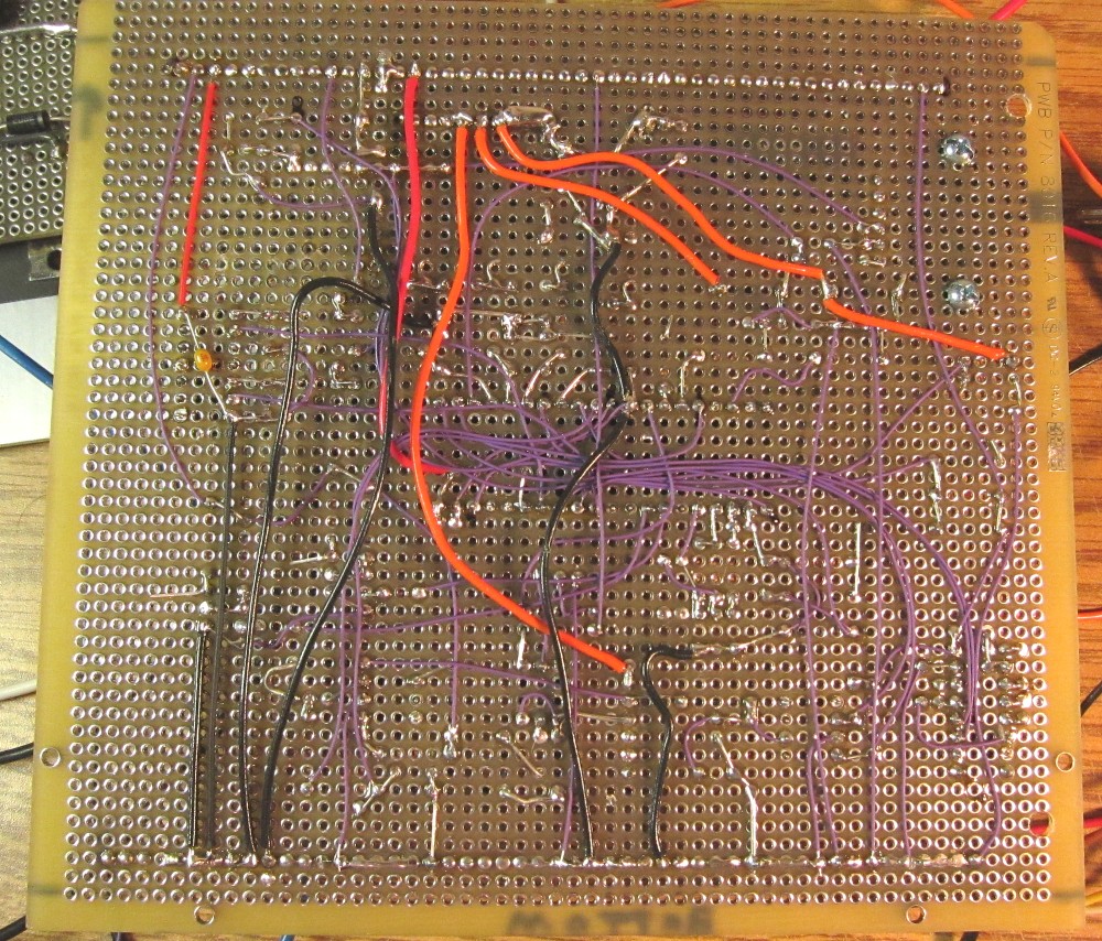
Progress pics. The sub-board has the power regulator along with all of the "noisy" stuff, which is basically the injector drivers and the IDL driver. They have their own dedicated grounds, completely isolated from the analog / logic grounds. (This is one of the design flaws in the 3.0 board that has always bothered me- everything shares a common ground.)
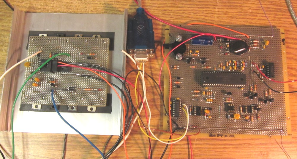
The backside is an homage to all of the hacked-on mods that have been done to MS1s over the years. I figure that if you're going to use some jumper wire, why not build the whole thing out of jumper wire?
Reply
1
1

 01-25-2012, 12:59 PM
#29
Boost Pope
Thread Starter
iTrader: (8)
Join Date: Sep 2005
Location: Chicago. (The less-murder part.)
Posts: 33,485
Total Cats: 6,898
I started by creating a full schematic, and then doing a capture into a PCB layout program. Even though I'm not planning to etch an actual PCB, I went ahead and designed it as though I were going to. I drew the PCB layout with most of the signal traces in place, and just put little stubs in place for the power and ground connections. Then I printed the layout at 1:1, both in normal view and in mirrored view (as it appears when looking at the backside.)
With this printout sitting on the desk, and the layout software running on a laptop, I'm just going through the board one pin at a time. Every time I run a jumper wire, I use a black sharpie to mark off the corresponding trace on the printout. So it's kind of like working off of a netlist, only in graphical form.
One wire at a time.
So far, the only error I have found is that while populating the board, I switched the positions of two resistors that were next to each other and formed a divider. Rather than pull them out and re-place them, I just compensated by reversing the wires on the backside.
You and me both.
Great Scott! I should have used 12AX7 vacuum tubes instead of PN2222A transistors!
I'll keep that in mind for the next build.
(Actually, now that I think about it, building an ECU with tubes in it would definitely get me a spot on Hackaday.com)
Aaaaw, what a cute little board.

Reply
0
0
 01-25-2012, 04:03 PM
#32
Elite Member

Join Date: Jul 2005
Posts: 6,420
Total Cats: 84
Progress pics. The sub-board has the power regulator along with all of the "noisy" stuff, which is basically the injector drivers and the IDL driver. They have their own dedicated grounds, completely isolated from the analog / logic grounds. (This is one of the design flaws in the 3.0 board that has always bothered me- everything shares a common ground.)
The trick is to keep the high current ground return paths completely separate from the analog small signal, sensor, and logic grounds, then you carefully think about the signals that have to cross those domains, e.g. MOSFET gate drives, in the face of differing ground potentials (can be as bad as 2V at high frequencies). The 2 grounds should only be connected to each other on the board via a polyfuse ("self resetting fuse" PTC thermistor) in case a user hooks up the grounds wrong and attempts to flow large ground return currents through the polyfuse. You also have to think about protection, what happens when 12V appears across this polyfuse. All engine sensor grounds should be connected to the ECU signal ground pin and nowhere else, not the chassis nor engine. The high current ground from the ECU should only carry the ground return currents of the high current drivers such as injectors, and power for the processor.
Reply
0
0
01-25-2012, 04:35 PM
#33
Boost Pope
Thread Starter
iTrader: (8)
Join Date: Sep 2005
Location: Chicago. (The less-murder part.)
Posts: 33,485
Total Cats: 6,898
then you carefully think about the signals that have to cross those domains, e.g. MOSFET gate drives, in the face of differing ground potentials (can be as bad as 2V at high frequencies). The 2 grounds should only be connected to each other on the board via a polyfuse ("self resetting fuse" PTC thermistor) in case a user hooks up the grounds wrong and attempts to flow large ground return currents through the polyfuse.
All engine sensor grounds should be connected to the ECU signal ground pin and nowhere else, not the chassis nor engine. The high current ground from the ECU should only carry the ground return currents of the high current drivers such as injectors, and power for the processor.
Looking at the factory wiring (this is a 1990 car), there are two wires (black) which are denoted as being for the high-current signals (2A "injector" and 2B "output") which both go to a common lug, and two other wires (black/grn) which are denoted as being for the low-current signals (2C "CPU" and 2D "Input") which go to a different common lug. These lugs attach to mounting brackets located at the aft end of the head and intake manifold. Ideally they would attach to the head itself (and I may still move them), but I suspect that this is probably good enough.
In the later cars, the analog sensor grounds actually go all the way into the ECU itself. In the 1.6 cars, the sensor grounds are bonded to the ECU "input" ground wire (the one from pin 2D) within the "front" harness, rather than looping all the way through the ECU.
By using the existing factory wiring I am somewhat limited in this regard, however by isolating the injectors and IDL drivers to the 2A / 2B grounds, and connecting the CPU board to the 2C / 2D grounds, I still plan to achieve a level of noise-immunity which is superior to that of a Megasquirt.
Reply
0
0
01-25-2012, 07:20 PM
#35
Elite Member
Join Date: Jul 2005
Posts: 6,420
Total Cats: 84
Looking at the factory wiring (this is a 1990 car), there are two wires (black) which are denoted as being for the high-current signals (2A "injector" and 2B "output") which both go to a common lug, and two other wires (black/grn) which are denoted as being for the low-current signals (2C "CPU" and 2D "Input") which go to a different common lug.
Reply
0
0
01-25-2012, 07:38 PM
#36
Boost Pope
Thread Starter
iTrader: (8)
Join Date: Sep 2005
Location: Chicago. (The less-murder part.)
Posts: 33,485
Total Cats: 6,898
Rather helpfully, the FSM diagram happens to have all of the major ECU-related grounds on the same page:
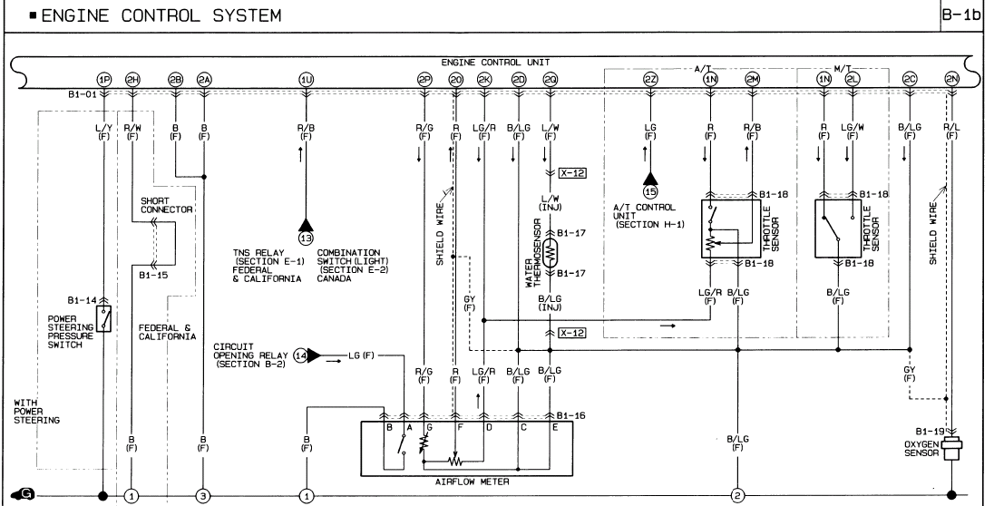
You can see the 2A / 2B grounds going to ground point 3 at the left of the screen, and the 2C / 2D grounds, along with the sensor and shield grounds, going to ground point 2 on the right half of the screen. Not shown on this page are the igniter ground, ignition condenser and ignition shield (which go to ground point 3 along with the other high-current stuff) and the CAS ground, which goes to ground point 2 along with the other low-level stuff.
It's an excellent design on Mazda's part, and fairly typical of what you find in most modern cars. Why the designer(s) of the rev 3.x Megasquirt board failed to take this into account when laying out their ground plane just absolutely flabbergasts me.
Reply
0
0

 01-25-2012, 08:32 PM
#38
Elite Member
Join Date: Jul 2005
Posts: 6,420
Total Cats: 84
Yeah, I thought I made that clear in the last post. The grounds for the analog sensors all join the black/green wires (the ones that goes from ECU 2C /2D to engine ground) within the "front" harness. I believe that all of these wires meet at junction point JC-02, which is inside the dashboard near the A/C evaporator, and then run from there to the engine, though I've never torn a 1.6 front harness apart to find out the exact routing.
Also, if you then keep your hi current ground completely separate from your logic/analog ground, then the return currents of MOSFET drive signals which cross these two realms, will have to travel down one ground wire to an engine lug, to the 2nd lug, then up the other ground wire. This can cause trouble. One solution is to situate Schmitt input signal conditioners before all MOSFETs, and to ground them to the MOSFET Source pins on your PCB (your high current ground). The signal inputs for these Schmitt triggers are then very noise immune, and the signal from your logic circuitry can tolerate a good deal of ground bounce between the 2 PCB grounds. Be sure to put some lopass filtering, the slowest that your signal can tolerate (e.g. 50 uS delay for injectors). Next you link the 2 ground systems on your PCB with a low value resistor (e.g. 2-20 ohms) so that there is a default path in case one ground wire is disconnected, and to provide a high frequency shunt (because the hi current ground wire will show lots of high frequency noise). Watch out tho, this shunt will cause some HF noise to couple into the sensor ground wire and appear as noise in the sensor signals. Note, it is always prudent to lopass all signals to the BW required. E.g. 10 us rise time on CKP, 20-50 ms rise times on MAP, 1 sec on temperatures.
Reply
1
1

 01-25-2012, 10:48 PM
#40
Boost Pope
Thread Starter
iTrader: (8)
Join Date: Sep 2005
Location: Chicago. (The less-murder part.)
Posts: 33,485
Total Cats: 6,898
I, too, was present for the first day of class in DC Circuits 1.

Also, if you then keep your hi current ground completely separate from your logic/analog ground, then the return currents of MOSFET drive signals which cross these two realms, will have to travel down one ground wire to an engine lug, to the 2nd lug, then up the other ground wire. This can cause trouble. One solution is to situate Schmitt input signal conditioners before all MOSFETs, and to ground them to the MOSFET Source pins on your PCB (your high current ground). The signal inputs for these Schmitt triggers are then very noise immune, and the signal from your logic circuitry can tolerate a good deal of ground bounce between the 2 PCB grounds. Be sure to put some lopass filtering, the slowest that your signal can tolerate (e.g. 50 uS delay for injectors). Next you link the 2 ground systems on your PCB with a low value resistor (e.g. 2-20 ohms) so that there is a default path in case one ground wire is disconnected, and to provide a high frequency shunt (because the hi current ground wire will show lots of high frequency noise). Watch out tho, this shunt will cause some HF noise to couple into the sensor ground wire and appear as noise in the sensor signals.
Note, it is always prudent to lopass all signals to the BW required. E.g. 10 us rise time on CKP, 20-50 ms rise times on MAP, 1 sec on temperatures.
On another note, at my last track event this guy came in with this baby full of ----. It was his "data" acquistion" board.
Reply
0
0


